Our Philosophy: Empowering Fast Research We believe that high-performance photonics should be accessible to everyone. Luxtelligence is committed to openness and collaboration, lowering the barrier to entry for next-generation optical innovation. By providing open access to our manufacturing rules, we empower you to focus on circuit design and accelerate your research.
Accelerate Your Design Flow Our Process Design Kits (PDKs) for LN-CORE™ (lnoi400) and LT-PRO™ (ltoi300) abstract away the process complexity.
Fast Research: Skip the process development phase with pre-validated components.
High Performance: Design with confidence, knowing our library is optimized for the low loss (< 0.2 dB/cm) and high bandwidth (> 110 GHz)
Community Driven: An open ecosystem that evolves with user feedback.
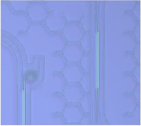
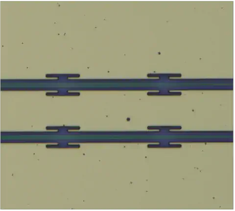
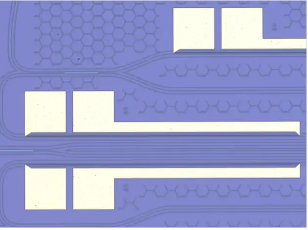
Validated Component Library Our PDKs include a suite of essential, pre-tested building blocks to streamline your layout.
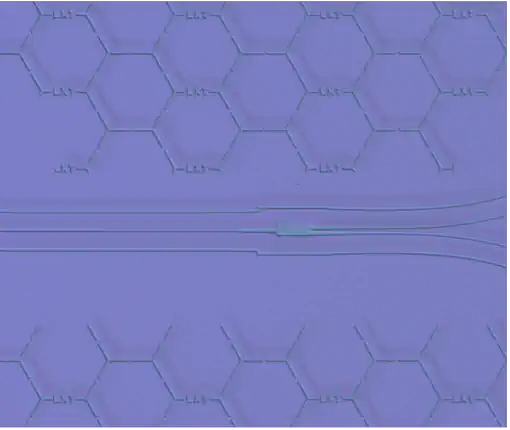
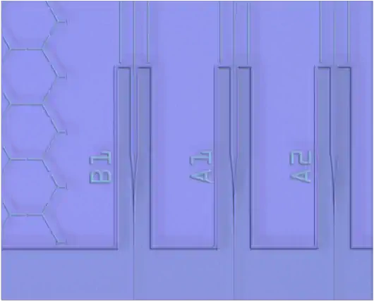
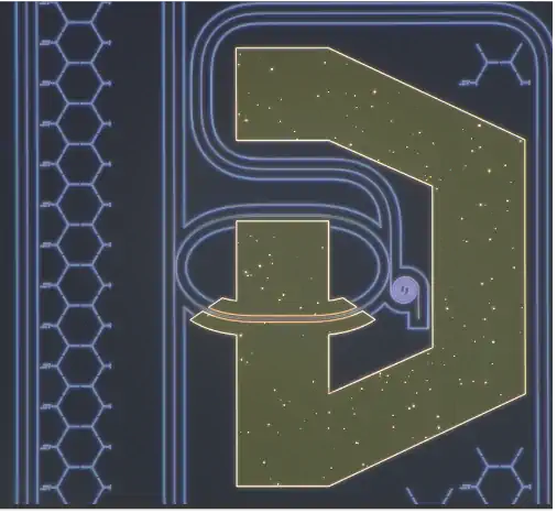
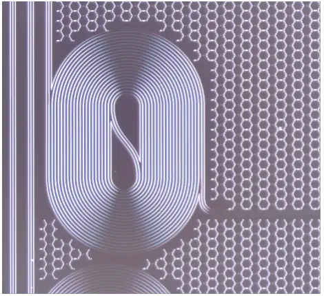
A selection of validated photonic components from our open-access PDK, including MMIs, edge couplers, thermal phase shifters (TOPS), microring modulators (MRM), traveling-wave Mach-Zehnder interferometers (TW MZI), and spirals.
We should show pictures of the devices. For all these pictures, we need to adjust the background to it merges well into the website background.
Check out our PDK on our github page!
Everything you need to know about our solutions
An MPW is a multi-project wafer run aimed at fast prototyping and design testing. Multiple clients submit their designs to the same batch and share the wafer space, which helps reduce costs while preserving their design secrecy. In this case, the vertical stack (i.e., the dimensions of the material layers) is fixed to the optimized value.
A DPW is a dedicated project wafer run where the whole wafer space is dedicated to the client, with the liberty to [choose the vertical stack? (we decided not change the stack?)] choose the die size and total number of wafers.
We perform our TFLT and TFLN fabrication runs on 4-inch wafers.
We are also in the process of transferring our fabrication to large volume foundries supporting 6-inch and 8-inch wafers. Please contact us for details.
For TFLT and TFLN MPW runs, the standard die size is 1 cm × 0.5 cm. There is also an option to reserve space for multiple dies and unify them into a single die, subject to an additional R&D cost. The extraordinary axis is aligned along the short dimension. The modulator electrodes and modulated waveguides are aligned along the long side of the die.
For DPW runs, the die size is flexible and is defined by mutual agreement prior to the start of fabrication.
You will receive at least 12 copies of your designed chip.
We can increase the number of chips by processing a supplementary wafer at additional cost.
We typically suggest starting with 2 wafers in a dedicated run with the ability of extending the batch up to [6-8 wafers (talk to Rui)] in the R&D cleanroom. Multiple batches can be ordered with shifted delivery times.
At the moment, we are transferring our fabrication process that can handle up to 10,000 wafers per month.
You can find the GDSFactory cells on our GitHub repository:
Our TFLT stack supports both the O-band and C-band components with high-resistivity terminations.
Our TFLN stack has only C-band components.
The client is free to suggest their own geometries. However, the minimal fabrication dimensions of 250 nm for waveguides and 800 nm for electrodes must be satisfied. A complete documentation with details on fabrication constrains is sent after signing an NDA.
You will receive a comprehensive design manual with examples and explanations. Upon availability, our engineers can provide certain fabrication and experimental data. Design consulting services are possible upon mutual agreement prior sending a purchase order.
After contacting LXT via the [contact form link], the client receives the MPW or DPW design manual. Once the purchase order (PO) is submitted, the design space is reserved and the client can begin their design.
To help minimize design errors, LXT provides multiple reference designs and examples on its open-source GitHub page.
The client must submit their completed design by the deadline published on the website for MPW runs, or by the mutually agreed deadline for DPW runs. Within two weeks following the submission deadline, LXT engineers perform a design rule check (DRC) and notify the client if any corrections are required.
After the design passes all checks, LXT proceeds with the fabrication process.
Our typical MPW lead time is 3 months for TFLN runs and 4-5 months for TFLT after the design rule check is complete. The DPW lead time depends on the number of requested wafers and complexity of the stack. Please contact our team for details.